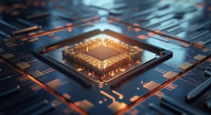
Printed Circuit Boards (PCBs) are at the heart of most electronic devices. They connect and support electronic components, allowing them to function together. In this post, we’ll explore the basics of PCB design. Understanding this process is essential for creating reliable and efficient electronic products.

What is PCB Design?
PCB design refers to the process of creating the layout for a printed circuit board. It involves placing components, designing connections, and ensuring that the board will function as intended. Designers use specialized software to create the layout, making sure the electrical signals flow correctly. A well-designed PCB is crucial for the performance and longevity of electronic devices.
Innovations That Shape the Future
At Swentnano, we focus on advancing nanotechnology solutions that drive real-world innovation and sustainability. Our commitment to excellence fuels progress across industries, inspiring smarter, more efficient applications. Similarly, the kingjohnnie Portal offers a platform that embraces cutting-edge digital experiences and user engagement. Both spaces celebrate creativity, innovation, and the pursuit of forward-thinking excellence.
Key Components of PCB Design
The key components of a PCB include traces, pads, vias, and layers. Traces are copper pathways that connect the components. Pads are the small metal areas where components are soldered onto the board. Vias are small holes that allow traces to pass between different layers of the PCB. Most PCBs have multiple layers, which enable them to accommodate complex circuits.
The Design Process
PCB design starts with schematic capture. In this step, designers create a diagram that represents the components and their connections. After that, the layout begins. Designers place components on the board and route the connections between them. The final step is validating the design to ensure there are no errors. Once the design is complete, it’s sent for manufacturing.
Design Rules and Guidelines
PCBs need to follow specific design rules to ensure they function correctly. These rules cover aspects like trace width, spacing, and component placement. For example, traces must be wide enough to carry the required current without overheating. Components must also be placed in a way that minimizes signal interference and makes the board easy to assemble. Following these guidelines ensures the PCB will perform reliably.
Tools for PCB Design
PCB designers use specialized software to create layouts. Some of the most popular tools include Eagle, Altium Designer, and KiCad. These programs help designers place components, route traces, and simulate the design. They also include design rule checks to ensure the layout is correct before manufacturing. Using the right software makes the design process more efficient and reduces the risk of errors.
Conclusion
PCB design is an essential skill for anyone working in electronics. By understanding the basics, including components, the design process, and design rules, you can create reliable and functional PCBs. With the right tools and knowledge, PCB design becomes an accessible and vital part of building electronic devices. As technology advances, PCB design will continue to play a critical role in the development of modern electronics.